Huawei Claims Chip Density Breakthrough by 2031
Is this a genuine innovation or a clever rebranding of existing industry techniques?
Story

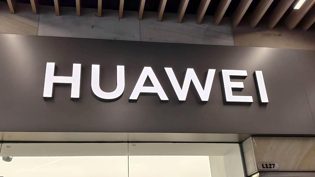
Above: A Huawei Smart Products Flagship Store in Shanghai, China, on May 21. Image credit: CFOTO/Future Publishing/Getty Images
The Facts
- Huawei claimed in Shanghai on Monday that its high-end chips will achieve transistor density equivalent to 1.4-nanometer processes by 2031, though the firm did not provide independent performance data.
- The announcement centers on a new design concept called the Tau Scaling Law, focused on reducing the time it takes signals and data to move through chips, and not shrinking transistors, an approach underpinning Moore's Law.
- Huawei's LogicFolding architecture, set to debut in Kirin smartphone chips this autumn, physically folds and stacks logic circuits into a dual-layer framework, which reportedly increases transistor density by 55% and power efficiency by 41%.


Sources Split
LEFT
CENTER
RIGHT
+1

+1
+1
+2

+2
ESTAB
CRIT
CENTER
PRO
ESTAB
The Spin
Narrative A
Huawei's Tau Scaling Law is a genuine leap forward for the semiconductor industry, replacing the dying framework of Moore's Law with a smarter, time-based optimization model. By 2031, Huawei's chips are on track to hit 1.4nm-equivalent density, proving this is a working industrial roadmap.


Narrative B
Huawei's Tau Scaling Law is savvy rebranding dressed up as a paradigm shift. Claiming 1.4nm equivalence by 2031 raises serious questions about what "equivalent" even means across density, performance and power. This process can inflate numbers without delivering a true generational leap.

Metaculus Prediction
Public Figures
The Controversies






© 2026 Improve the News Foundation. All rights reserved.Version 7.18.2
© 2026 Improve the News Foundation.
All rights reserved.
Version 7.18.2